အလင္း အာရံုခံ ဆင္ဆာေလးနဲ႕ အလုပ္လုပ္တဲ့ ဆားကစ္ေလးပါ.... မူရင္းေလးက ဒီလိုဗ်...
A light dependent resistor, LDR, could be used as part of a light sensor circuit. A tilt switch could be attached to the lid of the tin. Alternatively, you might attach a magnet to the lid of the tin and arrange for this to operate a magnetic switch (or reed switch). These devices would be part of a movement sensor subsystem.
Most alarms 'remember' that the sensor subsystem has been triggered. Closing the tin won't stop the alarm. A subsystem with this 'remembering' function is called a bistable, or latch.
Once you know the names and properties of the most important subsystems, you can use these building blocks to work out how to solve the design problem in outline.

How is this system going to work?
The sensor detects the opening of the tin. The output of the sensor triggers the latch so that its output goes HIGH. The reset subsystem provides some way of silencing the alarm.
An astable is a subsystem which produces pulses.
You may know about AND gates already. These follow a truth table where the output of the gate only becomes HIGH when both inputs are HIGH. ('HIGH' and 'LOW' in logic circuits always refer to HIGH and LOW voltages.)
AND gate truth table:
| input B | input A | output |
| 0 | 0 | 0 |
| 0 | 1 | 0 |
| 1 | 0 | 0 |
| 1 | 1 | 1 |
The AND gate is used in this system to decide whether pulses from the astable will be transferred to the audible warning device. If the output of the latch is LOW, no signals reach the audible warning device and the alarm is silent. On the other hand, if the circuit is triggered by opening the tin, the output of the latch becomes HIGH and the alarm sounds.
Work through the truth table of the AND gate to make sure you understand how this works.
Design Electronics includes details of all these subsystems. It's important to start building circuits straight away, so don't worry if you don't know about or understand everything all at once. For the moment, you need to concentrate on the skills involved in component identification, building prototype circuits, making measurements and soldering.
Sensor :
Sensor circuits almost always involve voltage divider circuits:

Which of these circuits gives an increase in Vout from LOW (logic 0) to HIGH (logic 1) when the tin is opened?

Which circuits give a decrease in Vout from HIGH (logic 1) to LOW (logic 0) when the tin is opened?
When the LDR is in the dark, substitute a big resistance, say 1 MW, in the formula. When the LDR is in the light, substitute a small resistance, say 1 kW. What size of resistance should be substituted when the tilt switch is closed?
Build a light sensitive voltage divider circuit on prototype board, as follows:

Confirm that this circuit gives a LOW voltage output when the LDR is exposed to light. There is a reason why you want a LOW output in the light which will become clear shortly.
Latch
One way of making a latch, also called a set-reset bistable, or set-reset flip flop involves two NAND gates. The symbol and truth table for an individual NAND gate are:

NAND gate symbol |
NAND gate truth table:
| input B | input A | output |
| 0 | 0 | 1 |
| 0 | 1 | 1 |
| 1 | 0 | 1 |
| 1 | 1 | 0 |
How does this differ from the truth table for AND?
Here is the circuit for a NAND gate latch:
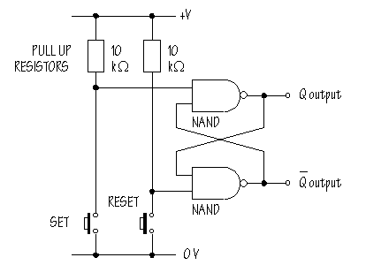
Pressing the SET button forces the Q-output to beome HIGH. The Q-output will stay HIGH until the RESET button is pressed.
To see what is happening, the NOT Q output can be used to drive an LED. Remember that LEDs need a series resistor to limit the current flowing:
driving an LED

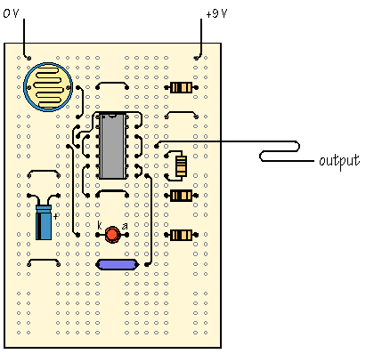
Change your prototype board circuit to include this circuit:

The latch circuit uses a 4093 Schmitt trigger NAND gate integrated circuit, with pin connections like this:

Look again at the circuit diagram of the latch and at the prototype board. Confirm that the links produce a pattern of connections on the prototype board which is identical to the the connections indicated by the circuit diagram.
Operate the SET and RESET switches. Write a sentence to describe the behaviour of the latch circuit:
Now modify your prototype board, using the LDR/voltage divider to replace the SET switch:

Cover the LDR with you hand. Press the RESET switch. What happens to the LED?
Now, uncover the LDR. What happens to the LED?
Cover the LDR once again. What happens to the LED?
Pressing RESET should make the LED go OFF. Uncovering the LDR should make the LED go ON. It should remain ON when the LDR is covered again. The latch 'remembers' that the circuit has been triggered.
How can you make the LED go OFF again?
You can arrange for the latch to be RESET automatically when the circuit is first switched ON. This is done using another voltage divider:

When the circuit is first switched ON, Vout is LOW because the capacitor is empty. The capacitor charges up slowly through the 1 MW resistor. If this resistor/capacitor combination is used to replace the RESET switch on the prototype board, you will find that the LED remains OFF for several seconds when the power supply is first connected:

If the LDR is covered during this time, the latch will not be triggered. The LED remains OFF until the LDR is suddenly uncovered.
This is exactly the behaviour you want for the biscuit tin alarm. When the battery is first connected, the power on RESET prevents the latch from being triggered. This is when you put the circuit into the tin and close the lid. Inside the tin, the capacitor charges up and the circuit becomes ready to operate, waiting for the hungry biscuit thief. As soon as the lid is opened . . .
Astable
Astables produce pulses. One of the simplest astable circuits needs just one resistor and one capacitor together with a Schmitt trigger NAND gate:
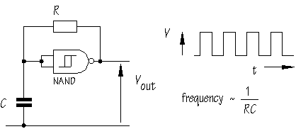
Add this circuit to your prototype board using a 10 kW resistor and a 100 nF capacitor:

You can monitor the output pulses using an oscilloscope, as indicated. The frequency of the pulses should be around 1 kHz, that is, one thousand pulses per second.
AND gate
In the original block diagram, the latch and astable outputs are both connected to the inputs of an AND gate. Pulses from the astable are transferred to the output of the AND gate when the output of the latch becomes HIGH. You can think of the latch as providing a control input which determines whether the astable pulses get through.
NAND gates can be used to control the transfer of astable pulses in a very similar way. Look at the circuit diagram:

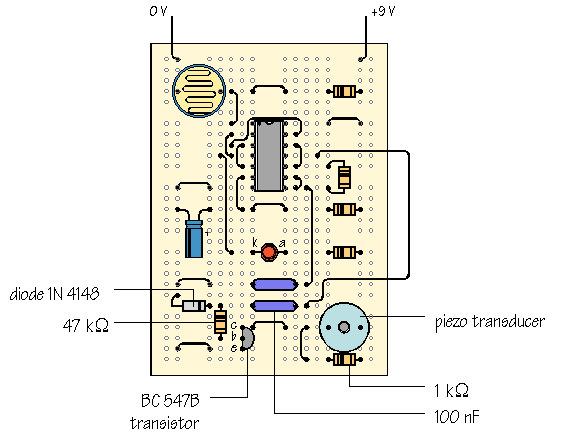
You have assembled most of the subsystems required by the block diagram. Modify your prototype board so that it looks like this:
Output
To complete the biscuit tin alarm, you need to add an audible warning device. This will be louder when driven via a transistor. The circuit is:

The transistor pin connections are:

Complete the circuit on prototype board as follows:
You have done extremely well if you have followed through the design process and built your biscuit tin alarm in prototype form. It is important to note that the development of the circuit is progressive. You start with just one subsystem on the prototype board and add further subsystems one at a time, testing the circuit and making modifications as you go along.
Final circuit
Prototype board testing leads eventually to a complete circuit for the device being developed. You can continue to make small alterations until the circuit behaves in the way you want.
The final circuit for the biscuit tin alarm is:
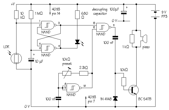
There are one or two alterations from the prototype board circuit you tested. A 10 kW preset resistor has been included. The resistance of the preset is adjusted using a screwdriver when the circuit is first assembled on printed circuit board and allows you to change the frequency of the astable pulses. This is useful because the piezo transducer oscillates more strongly at some frequencies than others. If you 'tune' the astable pulses to coincide with one of these resonant frequencies the noise produced is much louder.
A decoupling capacitor, 100 µF, has been added across the power supply. This helps to prevent the transfer of noise signals or 'spikes' along the power supply lines. It is good practice to include decoupling capacitors in your circuits. Do this even if you don't understand exactly what the capacitors are for!
Printed circuit board
Printed circuit board design involves locating the components which make up the circuit so that they can be easily soldered into the printed circuit board, or pcb, without wasting too much space. The pattern of copper tracks links the components together in the correct way.
Sometimes, the physical arrangement of components looks similar to the circuit diagram, so that you can work out which bit of the circuit is which. On the other hand, when the components are arranged around an integrated circuit ('beastie'), it can be difficult to identify different sections of the circuit. What matters is that the connections between components really are the same.
Designing printed circuit boards is a skill which you can learn. A good way to start is by looking carefully at the pcb's you use for your first soldered projects.
This is the printed circuit board design for the biscuit tin alarm:

Note that the track pattern for a pcb is usually visualised looking through the board as if it was transparent. This means that you can compare the component positions directly with the track layout.
 PCB available PCB available | Printed circuit boards for the biscuit tin alarm are available from DOCTRONICS. Please email for details. |
